1) Which among the following is a universal active filter?
a. Notch filter
b. All-pass filter
c. MF5 filter
d. Band pass filter
|
Answer
Explanation
Related Ques
|
ANSWER: MF5 filter
Explanation:
All the fundamental types of filters like low-pass, high-pass, band-pass, notch & all-pass filters can be easily designed with the help of MF% filter & hence, it is regarded as a universal filter. This MF5 is a second order filter which has the proficiency in realizing shape-desired response in addition to Butterworth, Chebyshev, Bessel & Elliptic. MF5 is also renowned as sampled data filter. Its one of the characteristic feature is that it can be cascaded so as to provide steep attenuation slopes.
|
|
2) The salient feature of sampled data systems is ______.
a. They affect signals at frequencies greater than twice the sampling frequency
b. They affect signals at frequencies greater than one-half the sampling frequency
c. They affect signals at frequencies lesser than twice the sampling frequency
d. They affect signals at frequencies greater than one-fourth the sampling frequency
|
Answer
Explanation
Related Ques
|
ANSWER: They affect signals at frequencies greater than one-half the sampling frequency
Explanation:
If a signal at frequencies greater than one-half the sampling frequency is applied to an input of sampled data systems, then it will get reflected to a frequency less than one-half the sampling frequency. This effect ultimately give rise to a phenomenon known as 'Aliasing Effect'. It is feasible to minimize or eliminate this effect by limiting the input signal spectrum to less than one half the sampling frequency.
|
|
3) Where does the series-pass transistor get switched in order to produce Pulse Width Modulation (PWM) in any series switching regulator circuit?
a. Between cut-off & saturation at high frequency
b. Between active & cut-off at high frequency
c. Between cut-off & saturation at low frequency
d. Between active & cut-off at low frequency
|
Answer
Explanation
Related Ques
|
ANSWER: Between cut-off & saturation at high frequency
Explanation:
Efficiency of a regulator can be increased by using series-pass transistor as a switch. The configuration arrangement of series switching regulator is in such a way that the series-pass transistor is allocated between cut-off and saturation region. This is so because it leads to the generation of square wave output representing pulse width modulation. Low pass LC filters the modulated square wave output so as to produce average DC output voltage. Since the output voltage is proportional to pulse width & frequency, the efficiency can be seen improved upto approximately 95%. These regulators find their applications in many kinds of circuits like push-pull, feed-forward and so on.
|
|
4) LM317 is a well-known ____.
a. Series-Switching Regulator
b. Series Dissipative Regulator
c. Special Regulators
d. None of the above
|
Answer
Explanation
Related Ques
|
ANSWER: Series Dissipative Regulator
Explanation:
LM317 is an adjustable & series dissipative regulator as they exhibit simulation of variable resistance between input and load. However, the mode of functionality is approved to be linear. These linear regulator are specifically designed to control or regulate constant output voltage by dissipation of excessive power in the form of heat when the input voltage and load current shows variations for certain extent. However, LM317 are considered as 'Series Dissipative Regulators'. The conversion efficiency in series dissipative regulator is inversely proportional to input/output differential value.
Thus, they are applicable to medium current applications where it becomes possible to manage dissipated power with heat sinks.
|
|
5) Which are the major key components are utilized by 8038 function generator according to monolithic technology?
a. Schottky-barrier Diodes
b. Thin-film Resistors
c. Both a & b
d. None of the above
|
Answer
Explanation
Related Ques
|
ANSWER: Both a & b
Explanation:
Monolithic components like Schottky-barrier diodes & thin-film resistors forms the basis for 8038 function generator. The main characteristic of Schottky diode is that it can perform the rectification for signal frequencies exceeding 300MHz. Besides this, thin film resistors are mainly built -up by using Silicon or alumina.
A very thin layer is deposited over the substrate of thin film resistor comprising two layers of conductivity and resistivity. However, though they are expensive but provides better electrical properties as compared to thick or any other kinds of resistors in the monolithic package.
|
|
6) Following are the specifications of _____.
a. Simultaneous Outputs: sine, square & triangular waves
b. Distortion: 1%
c. Operational Frequency: 0.001 to 500 KHz
d. Frequency Drift with temperature
a. LED Temperature Indicator
b. 555 Timers
c. 8038 Function Generator
d. Voltage Regulator
|
Answer
Explanation
Related Ques
|
ANSWER: 8038 Function Generator
Explanation:
8038 function generator is a 14-pin DIP which satisfies all the above mentioned specifications. LED temperature indicator, 555 Timers & voltage regulators consists of different configuration and specifications. It mainly comprises two comparators, two buffers, a flip-flop along with sine converter. These entire specifications are taken into consideration from an overall operational functions including 14 different pins.
Generation of triangular wave takes place by means of alternate charging the capacitor from one current source & then discharging it with another. This generated triangular wave is applied to both the comparators & then buffering becomes possible to sine converter. As a result, flip-flops and comparators play a significant role in converting triangular wave to square wave & also triangular wave gets converted to sine wave by means of sine converter.
|
|
7) Match the following pairs : Integration Levels Number of Components
a. SSI -------------------- 1. < 100 components
b. MSI ------------------- 2. > 1000 components
c. LSI -------------------- 3. < 10 components
d. VLSI ------------------ 4. > 100 components
a. A3, B1, C4, D2
b. A1, B4, C2, D3
c. A4, B2, C3, D1
d. A2, B4, C1, D3
|
Answer
Explanation
Related Ques
|
ANSWER: A3, B1, C4, D2
Explanation:
Classification of Integrated Circuits is based on the number of components mounted on the same chip inclusive of gates too. Number of components mounted on chip of Small-Scale Integration (SSI) are less than 10. If the number of components configured on a chip are less than 100, then the chip belongs to the category of Medium Scale Integration (MSI).
Apart from these, if the number of components goes on increasing the size of chip to about greater than 100, then the chip is associated with Large Scale Integration (LSI) whereas if the number of components exceeds than 1000, then the chip gets specified to the category of Very Large Scale Integration (VLSI).
|
|
8) By which name is non-inverting amplifier quite renowned due to its strategic functionality / mechanism?
a. Positive Scalar
b. Positive Vector
c. Negative Scalar
d. Negative Vector
|
Answer
Explanation
Related Ques
|
ANSWER: Positive Scalar
Explanation:
The necessity of using non-inverting amplifier arises whenever it is essential to obtain an output which should be equal to input with product of positive constant. Hence, it is also renowned by 'Positive Scalar' and this amplifier circuit utilizes negative feedback but along with the provision of desired output in terms of product of input as well as positive constant.
Negative Scaling is especially referred to 'Inverting Amplifier'. Remaining options mentioned above are meant for perplexities & has nothing to deal with non-inverting amplifier.
|
|
9) Which among the following is also used as a buffer or an isolation amplifier?
a. Inverting amplifier
b. Non-inverting amplifier
c. Unity Follower
d. Emitter Follower
|
Answer
Explanation
Related Ques
|
ANSWER: Unity Follower
Explanation:
Unity Follower circuit provides buffering or can be also used as an isolation amplifier which has a provision to obtain a gain at unity despite the requisite of any phase reversal. Emitter follower circuit is also semantic to unity follower only with an exception of gain which is in very much proximity of being absolutely equal to 1 (unity level).
Unity Follower is supposed to be used as buffer since it becomes quite feasible to transfer the input voltage in the form of output voltage along with the prevention of load resistance from loading down to input source simultaneously. This becomes possible because the value of input resistance tends to infinity & output resistance equals to zero.
|
|
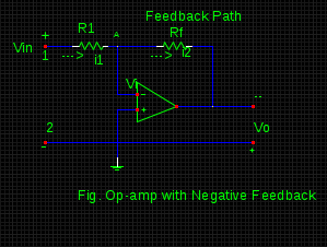
10) Why do the virtual ground strategy is adopted in case of Op-amps with negative feedback mechanism corresponding to the below figure?
a. Due to reduction in an input voltage at inverting terminal to zero
b. Due to reduction in an input voltage at inverting terminal to unity
c. Due to increase in an input voltage at inverting terminal greater than unity
d. All of the above
|
Answer
Explanation
Related Ques
|
ANSWER: Due to reduction in an input voltage at inverting terminal to zero
Explanation:
The notion of virtual ground originates from the condition when input voltage at the inverting terminal is insisted to reach a very minute value approximately to almost zero value. Thus, the point at which inverting terminal find its connection is significantly at the ground voltage and therefore, it is regarded at the virtual ground level. The reason behind getting reduction of input voltage to zero is the positive potential attained by point A and existence of the output voltage at the same time. Again, some part of output is fed back to input terminal out of phase. However, the sum of these two voltages become equal to zero.
|
|
11) According to figure, 'A' is referred as the summing point because of ______.
a. Addition of input and feedback currents at point 'A'
b. Addition of only input currents at point 'A'
c. Both a & b
d. None of the above
|
Answer
Explanation
Related Ques
|
ANSWER: Addition of input and feedback currents at point 'A'
Explanation:
Summing point is basically a point where all input as well as output or (may be feedback) are summed together. This point simply performs summation of all incoming currents coming towards it. In figure, point 'A' is a summing point. Since the configuration of Op-amp is exhibited to be of negative feedback in above drawn figure, so some part of output is connected at the input through point 'A' is also taken into consideration for the purpose of algebraic sum evaluation.
Generally, the concept of summing point and virtual ground are explained simultaneously for the semantic configuration requirement.
|
|
12) Which among the following amplifier circuit exhibit the output voltage in the form of phase inversion?
a. Adder
b. Substractor
c. Integrator
d. Differentiator
|
Answer
Explanation
Related Ques
|
ANSWER: Adder
Explanation:
In any adder circuitry of Op-amp, the output voltage must be equivalent to the summation of all input voltages where each input voltage is a multiple of constant gain factor. This circuit is usually more similar to inverting scalar type of amplifier with an exception of possessing more than one input. Therefore, output voltage of adder or summer Op-amp is phase inverted.
Referring to subtractor, integrator and differentiator amplifiers, the output voltage of subtractor deals with the difference between two input signals, while integrator generates its output voltage in terms of integral of input voltage whereas the output voltage of differentiator is proportional to change in input in accordance to time.
|
|
13) Which transistor is connected in parallel with feedback capacitor for termination of each ramp at a prescribed level in a Voltage Controlled Sawtooth Oscillator(VCO)?
a. BJT
b. FET
c. MOSFET
d. PUT
|
Answer
Explanation
Related Ques
|
ANSWER: PUT
Explanation:
Programmable Unijunction Transistor (PUT) is a switching device adopted by Op-amp integrator in VCO, which is generally connected in parallel to feedback capacitor so as to allow the termination of each ramp by adjusting reset conditions of the circuit. Thus, PUT comprises three terminals like an anode, a cathode and a gate where the biasing level of gate is supposed to be positive corresponding to the cathode.
An extravagant increase in an anode voltage as compared to gate voltage can be figured out by approximately 0.7 V. As a result, the PUT gets turn ON and starts operating like diode in forward biased stipulation. Thus, PUT gets turned OFF due to decrease in value of anode voltage below this level.
|
|
14) What is the purpose of notch filter?
a. To block all frequencies that fall within its bandwidth
b. To pass only limited range of frequencies irrespective of active filters
c. Both a & b
d. None of the above
|
Answer
Explanation
Related Ques
|
ANSWER: To block all frequencies that fall within its bandwidth
Explanation:
Notch filter mainly consists of a low pass filter, a high pass filter and a summing amplifier. The circuit configuration is in such a manner that cut-off frequency assigned by low-pass filter is lesser in value as compared to the cut-off frequency allocated by high-pass filter. Therefore, the gap between these both cut-off frequencies represents the bandwidth of the filter.
If the input frequency is lower than cut-off frequency of high-pass filter then output of high pass filter becomes zero. Hence, the total output of the filter will be equal to the output of low pass filter.
On the contrary, if the input frequency is higher than cut-off frequency of high pass filter, then output of low-pass filter tends to zero & hence, the net output under this condition will be definitely equal to the output of high pass filter.
As a result, it is perspicuous that notch filter permits to pass the frequencies below the cut-off frequency of low-pass filter and those above the cut-off frequency of high-pass filter, which can be termed as a crucial function or purpose of the notch filter.
|
|
15) The availability of Op-amps can be confined in _____.
a. Standard dual-in-line package (DIL)
b. TO-5 case
c. Flat-pack
d. All of the above
|
Answer
Explanation
Related Ques
|
ANSWER: All of the above
Explanation:
Designing of Op-amps is very crucial aspect since they need to be designed in such a way that external components should be connected to terminals so as to diverge or vary the external characteristics of Op-amps.
According to the technique of standard dual-in-line package, the ICs of Op-amp are sealed hermetically along with the two-sided packaging. Also, TO-5 case is well-known for 'Transistor Outline' and is concerned to a series of technical specifications. TO-5 type of packages belong to the header family metal case with the pitch of about 0.20'' via 90°.
Flat pack category of packaging mainly deals with PCB surface mount component packaging in the form of glass, metal or ceramics & hence provide greater defence to hermetic seals in order to prevent them from corrosion and moisture. Flat-pack type of packages are lighter and smaller as compared to the conventional round types of TO-5 cases.
All the three types mentioned above are highly confined for packaging dealt with Op-amps.
|
|
16) Which among the following Op-amps get manufactured by Semiconductor Limited, Pune?
a. CA 741 CT
b. CA 741 T
c. μ A 709
d. All of the above
|
Answer
Explanation
Related Ques
|
ANSWER: μ A 709
Explanation:
CA 741 CT & CA 741 T are the Op-amps developed or manufactured by Bharat Electronics Ltd (BEL), Bangalore. These are high-gain operational amplifiers which are absolutely applicable in summer, multivibrator, integrator, differentiator and so on.
μ A 709 is also a high-gain operational amplifier which is constructed on a single chip of silicon by an assistance of planar epitaxial mechanism by Semiconductors Limited, Pune. It's major areas of applications include DC servo systems, analog computers with high impedance values and low-level instrumentation prospects.
|
|
17) What will be the output voltage of an Op-amp inverting adder for the input voltages V1 = -10V, V2 = +10V, V3 = +5V and resistances R1 = 600K Ω, R2 = 3000K Ω & R3 = 2M Ω if the feedback resistance is considered to be 2M Ω?
a. -38.3V
b. 38.3V
c. 40V
d. -40V
|
Answer
Explanation
Related Ques
|
ANSWER: -38.3V
Explanation:
Given data:
V1 = -10V, R1 = 600k
V2 = 10V, R2 = 300K
V3 = 5V, R3 = Rf = 2M
The output voltage of an inverting adder or summer circuit is evaluated by,
Vo = -(K1V1 + K2V2 + K3V3)
where, 'K' represents the constant gain factor.
K1 = Rf / R1 = 2M/ 600K = 2000K/ 600K = 3.33
K2 = Rf / R2 = 2M/300K = 2000K/ 300K = 6.66
K3 = Rf / R3 = 2M/ 2M = 1
Therefore, Vo = -(K1V1 + K2V2 + K3V3)
= -[3.33 x (-10) + 6.66 x (10) + 1 x 5]
= -[-33.3 + 66.6+ 5]
= -38.3 V
Hence, the final output value of voltage of an inverting amplifier is nothing but summation of all input voltages estimated to be in terms of negative voltage of about -38.3 V.
|
|
18) An increase in operating frequency also increases ______ between input and output and decreases ______ for a compensating network of an amplifier.
a. Phase shift & magnitude (gain)
b. Phase shift & break frequency
c. Magnitude (gain) & Phase shift
d. Break frequency & Phase shift
|
Answer
Explanation
Related Ques
|
ANSWER: Phase shift & magnitude (gain)
Explanation:
It is the fundamental property of an amplifier that the value of gain (magnitude) goes on decreasing while phase-shift between input and output goes on increasing whenever there is rise in an operating frequency.
Change in the gain of an Op-amp due to variation in frequency is graphically estimated by 'Magnitude Plot', whereas change in phase with respect to variation in phase-shift is evaluated in terms of 'Phase Angle Plot'.
However, modification in an op-amp performance can be handled as per the requisite level by controlling the level of gain and phase-shift of the compensating networks.
|
|
19) Which among the following are the major responsible reasons for the cause of 'Slew Rate'?
a. Current limiting
b. Saturation of internal stages due to application of high frequency & amplitude signal
c. Both a & b
d. None of the above
|
Answer
Explanation
Related Ques
|
ANSWER: Both a & b
Explanation:
Slew rate is the maximum rate of change of output voltage with respect to time. For an instance, suppose that if the slew rate appears to be 1V/microseconds, then the output rises or falls at the speed rating of 1V/microseconds. Slew rates are also referred as output voltage swing as a function of frequency or as a voltage follower large signal pulse response. Also, the slew rate has an inverse relation to temperature. As the temperature increases, the slew rate decreases.
Since slew rate belongs to the category of large signal phenomenon, current limiting and the saturation of intrinsic stages of op-amp leads to reasons of slew rate to greater extent. However, when a frequency & amplitude signal is applied, the resulting current is also at extravagant level so as to charge the network of capacitance compensation. It is obvious that charging & discharging of capacitor needs some finite amount of time and therefore, the internal capacitors are solely responsible in preventing the output voltage to respond instantaneously to the fast varying input.
Hence, capacitor charging rate affects the current limiting in slew rate, which indicates that the voltage across the capacitor is nothing but the output voltage.
|
|
20) Which of the following AC parameters of an Op-amp results in reduction of output voltage if it becomes excessive?
a. Transient Response
b. Slew Rate
c. Bandwidth
d. All of the above
|
Answer
Explanation
Related Ques
|
ANSWER: Bandwidth
Explanation:
The significant AC parameters of Op-amp are transient response, bandwidth and slew rate but all of them have different results while becoming excessive. The transient response affects the settling time while slew rate give rise to distortion if exceeded. As a result, bandwidth reduces the output voltage when it is exceeded.
Since bandwidth is a small signal phenomenon, it represents the band of frequencies for which the gain remains constant & also highly dependable on compensating components including closed loop gain. But, it exhibits adverse consequences in the reduction of an output voltage when exceeded to greater extent.
|
|
21) What is the connection configuration of swamping resistor in case of a differential amplifier?
a. In series with each emitter
b. In series with each collector
c. In parallel with each collector
d. In parallel with each emitter
|
Answer
Explanation
Related Ques
|
ANSWER: In series with each emitter
Explanation:
External resistor of a differential amplifier is connected in series combination with each emitter. Due to this configuration, the dependability of voltage gain which varies in accordance to changes in emitter resistance can be ablated. Apart from this advantage, external resistor also possesses a beneficiary notion of increasing the linearity range of differential amplifiers.
However, the value of external resistor has an efficiently high value to swamp the consequences of emitter resistor of amplifier. As a result, this external resistor is also renowned as 'Swamping Resistor' because of its swamping strategy.
|
|
22) Which transistor array is essential in construction of a mirror circuit where the formation of diode takes place by an adjacent transistor?
a. CA3081
b. CA3046
c. CA3086
d. CA3083
|
Answer
Explanation
Related Ques
|
ANSWER: CA3086
Explanation:
CA3086 play a significant role in proper execution or operation of the circuit during the construction of mirror circuit. Here, the diode gets formed with an assistance of transistors placed adjacently. However, this type of transistor array ultimately leads to acquire the thermal stability and the requisite amount of collector current in a current mirror circuit.
Due to simplicity in fabrication and operation, current mirror circuit have wide range of applications in the aspects of differential and operational amplifiers.
|
|
23) The below drawn schematic of Op-amp 741 is configured in non-inverting mode with R1 = 2 K Ω, Rf = 20 K Ω, fo = 10 Hz & A = 4,00,000. Determine the following parameters :
1) Af
2) fF
a. 10.99 & 90.9 kHz
b. 10.99 & 36.36 kHz
c. 10.99 & 20 kHz
d. 10.99 & 10 kHz
|
Answer
Explanation
Related Ques
|
ANSWER: 10.99 & 36.36 kHz
Explanation:
For non-inverting mode of an amplifier (voltage series feedback amplifier)
1) Af = AB / 1 + AB
But, B = R1 / (R1 + Rf) = 2 k / (2 k + 20 k)
= 1 / 11
1 + AB = 1 + 400000 x (1 / 11)
= 36364.6
Af = 400000 / 3636.4 = 10.99
2) fF = (1 + AB) fo = (36364.6) x 10Hz = 363646 = 36.36 KHz
|
|
24) What will be the designing components for designing second order low pass filter at a high cut-off frequency of 1kHz assuming C = 0.0047μ F along with consideration of standard pot values?
a. R2, R3 = 33k Ω, C1 = C2 = 0.0047μ F, R1 = 27k Ω & Rf = 15.8k Ω
b. R2 = R3 = 66k Ω, C1 = C2 = 0.0047μ F, R1 = 35k Ω & Rf = 60k Ω
c. R2 = R3 = 51k Ω, C1 = C2 = 0.0047μ F, R1 = 67k Ω & Rf = 70k Ω
d. None of the above
|
Answer
Explanation
Related Ques
|
ANSWER: R2, R3 = 33k Ω, C1 = C2 = 0.0047μ F, R1 = 27k Ω & Rf = 15.8k Ω
Explanation:
Since the value of high cut- off frequency is mentioned. Below enlisted are the steps to evaluate filter components of second order low pass filter for designing purpose.
Step 1 : Assume R2 = R3 = R & C1 = C2 = C.
Step 2 : Select the value of C = 1μ F
Suppose that C1 = C2 = C = 0.0047μ F
Step 3 : Determine R by using formula R = 1 / 2 π fH C
R2 = R3 = 1 / (2 π x 103 x 47 x 10-10)
= 33.86k Ω
(consider the round figure value i.e. 33k Ω
As we know that Rf should be equal to 0.586 x R1, then R1 = 27k Ω)
Thus, Rf = 0.586 x 27 = 15.86k Ω
By taking into consideration the pot value of about 20k Ω, estimated resistances are
R2 = R3 = 33k Ω
C2 = C3 = 0.0047μ F
R1 = 27k Ω & Rf = 15.8k Ω
Step 4 : Since the values of resistors and capacitors are equal , the passband voltage gain must be equal to Af = 1 + (Rf / R1) 1.586
However, the gain must satisfy the Butterworth response & hence, the value of R1 must be selected = 100k Ω in order to estimate the value of Rf.
|
|
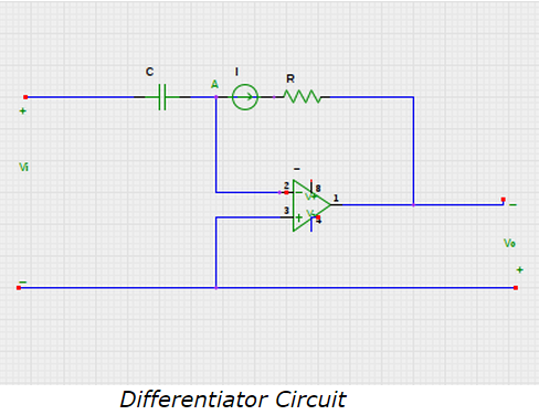
25) What will be the output of differentiator circuit if input sinusoidal voltage has a peak value of 7mV & frequency of 1KHz when the values of resistance and capacitors are R = 1500K and C = 2μF respectively?
a. -1000 π cos 2000 πt
b. -2000 π cos 2000 πt
c. -42000 π cos 2000 πt
d. -21000 πcos 2000 πt
|
Answer
Explanation
Related Ques
|
ANSWER: -42000 π cos 2000 πt
Explanation:
Given data:
Voltage Peak Value = 7mV
Frequency = f = 1KHz
R = 1500K Ω
C = 2μF = 2 x 10⁻⁶ F
An input voltage equation of a differentiator circuit can be expressed by,
V1 = Asin2 πft
= 7 sin2π x 1000 t
= 7 sin2000π t mV
Scale Factor = -CR = - [2 x 10-6 x 15 x 105]
= - [30 x 10-1 ]
= -3
Hence, the output voltage of differentiator circuit can be evaluated as:
Vo = -3 d / dt [7 sin 2000 π t]
= -3 x 7 x 2000 cos 2000 π t
= -42000 π cos 2000 π t mV.
|
|
26) What will be the values of bandwidth & maximum output voltage swing respectively in an non-inverting amplifier with input resistance of about 40 ohm, input capacitance of about 0.1μF with inclusive of R1=R2=R3=200K Ω, Rf = 2M Ω and Vcc = + 20V?
a. 32.56 kHz & 20 Vpp
b. 30.56 kHz & 20 Vpp
c. 47.56 kHz & 20 Vpp
d. 67.56 kHz & 20 Vpp
|
Answer
Explanation
Related Ques
|
ANSWER: 47.56 kHz & 20 Vpp
Explanation:
In accordance to given data, the ac input resistance of the amplifier can be given by,
Rif = (R2)¦(R3)¦ [Ri (1+AB)]
When [Ri (1+AB)] >> R2 or R3 then, the above equation becomes
Rif ≈ (R2)¦(R3)
≈ 200K ¦ 200K
= 100K Ω
The low frequency cut-off limit can be exaggerated using
fL = 1 / [2 πCi(RiF + R0)]
= 1 / [2 π (0.1 x 10 -6) (100K +40 )]
= 62.8 Hz
The gain of an amplifier is = 1 + (Rf / R1)
= 1 + (2M / 100K)
= 21
From the formula of Unity gain bandwidth,
UGB = Af x FH
Therefore, fH = UGB / Af = 1 M / 21 = 47.61 Khz
Bandwidth = FH – FL = 47.61 Khz – 0.0476 KHz = 47.56 KHz &
Ideal Maximum Output Voltage Swing = +Vcc = +20Vpp.
|
|
27) Determine the values of load current and output voltage respectively for the below schematic of voltage to current converter with grounded load by assuming that the op-amp is nulled at the inception.
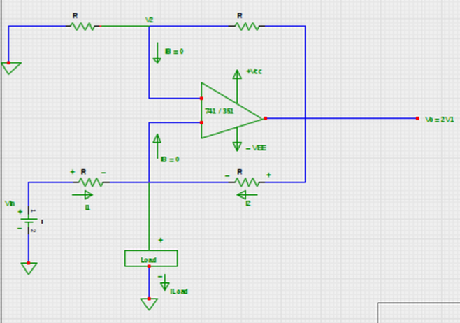
a. 0.3 mA & 4V
b. 30 mA & 4V
c. 300 mA & 2V
d. 30 mA & 2V
|
Answer
Explanation
Related Ques
|
ANSWER: 0.3 mA & 4V
Explanation:
Given data :
From the circuit, the given values are:
Vin = 10V, R = 30K & V1 = 2V
We know that load current depends on input voltage resistance R in case of voltage to current converter.
Thus, IL = Vin / R
= 10V / 30K
= 0.3 mA
However, the output voltage (Vo) of voltage to current converter is given by,
Vo = 2 V1 = 2 x 2 = 4V.
|
|
28) For the circuit shown below, +V = 15V, R2 = 1K, R1 = R3 = 8K & C1 = 0.001μF. Compute
(a) nominal frequency of output waveforms &
(b) Modulation in the output frequencies if Vc changes in the mist of 10V to 11.5V.
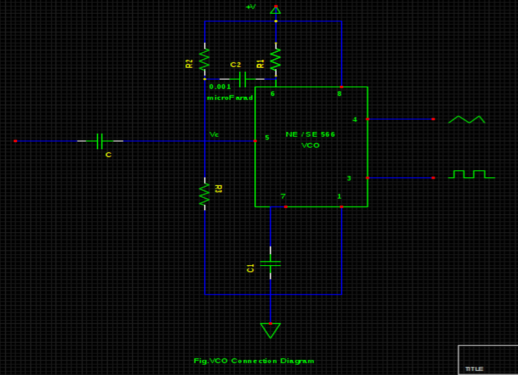
a. 26.17 & 33.34 kHz
b. 35.60 kHz & 10 kHz
c. 30.47 kHz & 10 kHz
d. 22.56 & 33.34 kHz
|
Answer
Explanation
Related Ques
|
ANSWER: 30.47 kHz & 10 kHz
Explanation:
(a) By applying voltage -divider rule, initial voltage at terminal 5 is given by,
Vc = (20K) (15) / 11.5K = 26.09 V
Thus, the frequency of output waveform (nominal frequency) is approximated by,
fo ≈ 2(+V - Vc) / R1C1 (+V)
= 2 (15 – 10.43) / (20K x 10-9) x (15)
= 30.47 kHz
(b) Thus, the modulation in the output frequencies can be calculated by initially substituting Vc = 10V & then 11.5 V
fo = 2 (15 – 10) / 20K x 10-9 x 15
= 33.34 kHz
fo = 2 (15 – 11.5) / 20K x 10-9 x 15
= 23.34 kHz
Hence, the variation in an output frequency can be evaluated by the difference between these both frequencies.
i.e. 33.34 - 23.34 = 10 kHz.
|
|
29) Which among the following parameters is usually only specified in dual and quad level Op-amps which is precisely known as amplifier to amplifier coupling?
a. Average Temperature coefficient
b. Channel Separation
c. Gain-Bandwidth Product
d. Offset V & I Stability
|
Answer
Explanation
Related Ques
|
ANSWER: Channel Separation
Explanation:
Channel separation is a measure of the amount of electrical coupling between the op-amps which are integrated on a semantic chip. This parameter is specifically highlighted in datasheet specifications of dual & quad Op-amps like μAF772 & μAF774 respectively.
Whenever there is an application of signal to input of only one op-amp, then some of the other signal appears on the output confined level of other op-amps due to physical vicinity of op-amps in dual and quad form of packages.
However, the amplitudes of all these signal are almost similar and therefore, can be evaluated with an assistance of channel separation. This conceptual characteristic of parameter specification & mechanism is supposed to be referred as 'amplifier to amplifier coupling'.
|
|
30) The cardinal characteristics of BJT in terms of applicable functionalities include____.
a. Linear amplification
b. Boosting of an electrical signal
c. Act as an electronic switch
d. All of the above
|
31) Which region / terminal of BJT undergoes through the phase of heavy doping in accordance to the function associated with the supply of majority charge carriers to base of transistor?
a. Emitter
b. Base
c. Collector
d. All of the above
|
32) Why is the collector region of transistor made larger as compared to emitter region from the physical spacing point of view by reducing the probabilty of transistor inverting?
a. For maintenance of requisite amount of doping level
b. For maintenance of similar polarity with respect to base
c. For maximum power dissipation
d. For maximum allowance of current flow
|
33) Which statements approves to be precise in case of FR biasing for normal working strategy and operation of transistor?
A. Emitter-base junction must be forward biased
B. Collector-base junction must be reversed biased
C. Emitter-base junction must be reversed biased
D. Collector -base junction must be forward biased
a. A & C
b. A & B
c. B & D
d. C & D
|
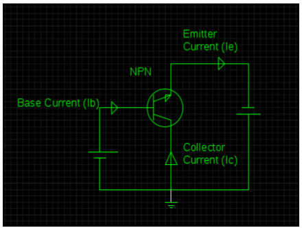
34) The common -base mode configuration of PNP transistor relates the direction of current flow and associated magnitude in terms of overall current supply equation as _____.
a. IE = IB + IC
b. IE = IB - IC
c. IE = (IB + IC) / 2
d. IE = (IB - IC) / 2
|
35) Current generation to small extent takes place in transistor because of minority charge carriers irrespective of the majority charge carriers can be termed as _______.
a. Recombination Current
b. Collector Junction Current
c. Emitter Junction Current
d. Leakage Current
|
36) The mode of representing the potential difference between emitter and base is always designated as VEB despite of VBE since ______.
a. base is positive w.r.t emitter
b. base is negative w.r.t emitter
c. emitter is positive w.r.t. base
d. emitter is negative w.r.t base
|
37) Which parameter signifies the quality measure ratio of collector to emitter current in CB configuration of transistor that is almost regarded as an equivalent form of forward current transfer ratio?
a. Alpha (αdc)
b. Beta (βdc)
c. Gamma (γ)
d. None of the above
|
38) Which type of transistor circuit configuration/s yields the phase-shift of about 180 °?
a. CC
b. CB
c. CE
d. All of the above
|
39) The resemblance of amplification factor in CE configuration can be discovered equivalent to h-parameter value of ______.
a. hie
b. hre
c. hfb
d. hfe
|
40) Compute the value of output current for the schematic diagram of CC configuration if IB = 15μA with an amplification factor of 400.
a. 6.01 mA
b. 7.01 mA
c. 8 mA
d. 10 mA
|


