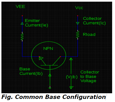
1) The collector to base current with emitter open circuit configuration in CB mode is extensively dependent on temperature as a result of ________.
a. Thermally generated minority carriers
b. Thermally generated majority carriers
c. Thermally generated majority as well as minority carriers
d. None of the above
|
2) The phenomenon of thermal runaway occurs due to maximum and simultaneous increase in power dissipation and _________ beyond safe operating value which ultimately results in causing damage to transistor.
a. Collector Current
b. Emitter Current
c. Base Current
d. All of the above
|
3) What is the value of base current if the common base circuit configuration offers an emitter current of 3 mA, collector current of 1.5 mA along with the reverse saturation current is 11 mA?
a. 1.5 mA
b. 3 mA
c. 0.15 mA
d. 0.20 mA
|
4) The greater level of signal distortion that can be managed by transistor can be visualized in the input static characteristics of common base configuration due to variation in input resistance with respect to ________.
a. Base to emitter voltage
b. Base to collector voltage
c. Base to base voltage
d. None of the above
|
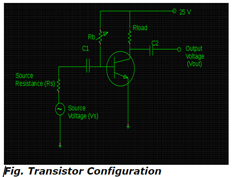
5) Which type of connection/s is/are rarely employed for audio-frequency circuits due to assortments in input & output resistances in addition to current gain less than unity?
a. CC
b. CB
c. CE
d. All of the above
|
6) The output or collector characteristics of common emitter configuration exhibits variation in VCE due to variation in IC by maintaining _______.
a. IE constant
b. IB constant
c. VBE constant
d. VBB constant
|
7) What value of load resistance (RL) generates collector to base voltage (VCB) of about 6V for the following circuit configuration?
a. 14k Ω
b. 12k Ω
c. 10k Ω
d. 8k Ω
|
8) Which rule clarifies an ideology of referring the resistance from one part of transistor to another of its parts similar to the strategy of using primary & secondary winding impedances of a transformer?
a. Alpha rule
b. Beta rule
c. Gamma rule
d. None of the above
|
9) It is possible to determine the operating state of transistor with an assistance of VCE under the category of well into saturation region if value of VCE is______.
a. only greater than zero
b. only equal to zero
c. only less than zero
d. greater than or equal to zero
|
10) The saturation condition of transistor implies that _______.
a. Collector current has highest possible value
b. Entire Vcc gets dropped across load resistor
c. It acts as a closed switch with negligible value of resistance
d. All of the above
|
11) What is an essential possible condition of biasing for a transistor to operate in an active region?
a. Forward biasing of emitter base & collector base junctions
b. Reverse biasing of emitter-base & collector-base junctions
c. Forward biasing of emitter base & Reverse biasing of collector-base junctions
d. Reverse biasing of emitter-base & Forward biasing of collector-base junctions
|
Answer
Explanation
Related Ques
|
ANSWER: Forward biasing of emitter base & Reverse biasing of collector-base junctions
Explanation:
No explanation is available for this question!
|
|
12) Which operating condition is satisfied by the transistor if it is supposed to function in cut-off region?
a. VCE > 0
b. VCE = 0
c. VCE < 0
d. VCE = Vcc
|
13) Which operating region of BJT enables Emitter-base & Collector-base junctions to undergo perfect short-circuit configuration?
a. Active Region
b. Saturation Region
c. Cut-off Region
d. None of the above
|
14) Which current source is connected between collector and base terminals in order to supervise the consequences of base control in an active region DC Model of BJT?
a. αIB
b. βIB
c. αIE
d. βIE
|
15) The current source acting as a function of variable in N-P-N transistor DC model is renowned as _______.
a. Dependent Source
b. Controlled Source
c. Both a & b
d. None of the above
|
16) Which functional mode enables the BJT to act as an open switch under the application of zero input control signal?
a. BE junction only in forward biased mode
b. BE junction only in reversed biased mode
c. BE junction in forward as well as reversed biased mode
d. None of the above
|
17) It is possible for a transistor to act as a closed switch by defining requisite magnitude of saturation level with an equivalent amount of ______.
a. Positive control voltage
b. Negative control voltage
c. Both positive & negative control voltages
d. None of the above
|
18) What should be the desirable stipulated form of relationship between VCE & Vcc for a transistor to function as an amplifier?
a. VCE should be half of Vcc
b. VCE should be double of Vcc
c. VCE should be one-third of Vcc
d. VCE should be four times the value of Vcc
|
19) What is/are the possible phases of operational configuration when VCE becomes exactly equal to Vcc in accordance to the considerations of fault location strategy of transistor?
a. Acts as an open-circuited configuration
b. Operates especially in cut-off region
c. Connection all resistors in series combination by keeping VCE as shorted
d. All of the above
|
20) What are the values of Vc & VE respectively for the circuit diagram displayed below?
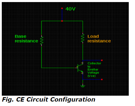
a. 15 V & 20 V
b. 20 V & 10 V
c. 30 V & 10 V
d. 40 V & 20 V
|
21) What should be the combined value of resistance according to Beta rule especially when the value of βRE is greater than R2 in the following schematic configuration of Universal Stabilization Circuit?
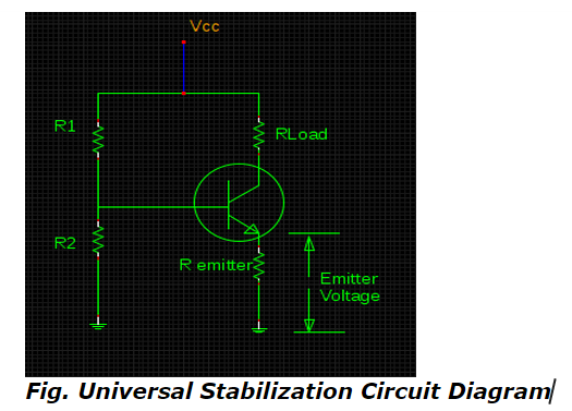
a. R2 ¦ βRE
b. R2 ¦ βRL
c. R1R2 ¦ βRE
d. R1R2 ¦ βRL
|
22) What does the notation of VBB ↓ , IB ↓ , IC ↓ , IC RL ↓ , VCE ↑ imply, according to the notation rules at incremental & decremental stages?
a. Decrease in input voltage increases the output voltage
b. Increase in input voltage decreases the output voltage
c. Increase in input voltage also increases the output voltage
d. Decrease in input voltage also decreases the output voltage
|
Answer
Explanation
Related Ques
|
ANSWER: Decrease in input voltage increases the output voltage
Explanation:
No explanation is available for this question!
|
|
23) Which is the standard form of representing the instantaneous values of AC currents in accordance to V-I notation rules?
a. IE, IB, IC
b. ie, ib, ic
c. Ie, Ib, Ic
d. All of the above
|
24) Which device plays a significant role in connection of ac source without affecting or causing any sort of perturbation to dc biasing while applying AC to DC biased transistor?
a. Inductor
b. Resistor
c. Coupling Capacitor
d. Filter
|
25) What is the phase angle difference between ac output and input voltages corresponding to AC/DC analysis of transistor?
a. 90° in phase with each other
b. 90° out-of-phase with each other
c. 180° in phase with each other
d. 180° out-of-phase with each other
|
26) Compute the value of VCE for the following circuit by taking into consideration the standard values of Av = β = 100 along with peak input signal voltage of about 0.03V
a. 3.75 A
b. 5.75 A
c. 3.25 A
d. 5.25 A
|
27) It is feasible to draw DC load line of a transistor with an acquaintance of _____ points.
a. Cut-off & saturation
b. Active & cut-off
c. Active & saturation
d. All of the above
|
28) Which point on the DC load line exhibit collector current and collector-emitter junction voltage that gets emerged in a transistor even without an application of input signal?
a. DC operating point
b. Quiescent Point
c. Working Point
d. All of the above
|
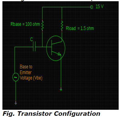
29) What is the value of base resistance if the values of β & VBE are assumed to be 40 & 0.7V respectively in order to obtain the operating point in the following schematic diagram ?
a. 965 Ω
b. 972 Ω
c. 985 Ω
d. 962 Ω
|
30) Which biasing method acquires better stability of dc operating point against the variations in β with an assistance of emitter resistor eventually leading to degeneration?
a. Base bias with emitter feedback
b. Base bias with collector feedback
c. Emitter bias with two supplies
d. Fixed current bias
|
31) What is the value of stability factor for CB circuit configuration?
a. S = 1 + β
b. S = 1 - β
c. Zero
d. Unity
|
32) Universal form of biasing with single supply applicable in several linear discrete circuits to greater extent is regarded as the fundamental form of ________.
a. Base biasing
b. Fixed current biasing
c. Voltage divider biasing
d. None of the above
|
33) The shifting of Q-point in upward and downward directions with respect to the variations in output voltage and current of an amplifier is the major characteristic feature of _______.
a. DC Load Line
b. AC Load Line
c. Both a & b
d. None of the above
|
34) Which equation represents the slope of an AC Load Line?
a. y = -1 / Rac
b. y = 1 / Rac
c. y = -1 / RL
d. y = 1 / RL
|
35) Which statement regarding AC & DC load lines approves to be correct?
a. AC load line is steeper than DC load line
b. DC load line is steeper than AC load line
c. Both AC & DC load lines are equally steeper
d. None of the above
|
36) Which transistor is also renowned as 'Insulated Gate Field Effect Transistor' (IG-FET)?
a. Junction FET
b. Metal-Oxide Semiconductor FET
c. Both a & b
d. None of the above
|
37) Which are the majority charge carriers in P-channel JFET by enhancing the flow of current between two N-regions or gates?
a. Holes
b. Electrons
c. Both a & b
d. None of the above
|
38) Which internally connected region is heavily doped with an impurity by forming double PN junctions in JFET?
a. Source
b. Drain
c. Gate
d. Channel
|
39) The passage of majority charge carriers from source to drain terminal takes place through the channel only after an application of
a. Drain to Source Voltage (VDS)
b. Gate to Source Voltage (VGS)
c. Gate to Gate Voltage (VGG)
d. Drain to Drain Voltage (VDD)
|
40) According to the symbolic representation of N & P channels, the gate arrow is always pointed towards ______.
a. P-type material
b. N-type material
c. P-type in p-channel FET & N-type in n-channel FET
d. All of the above
|


