1) On the application of VDD to JFET, the biasing strategy of gate to channel at any point over the channel yields output equal to _______.
a. Numerical sum of VDS & VGS
b. Numerical difference of VDS & VGS
c. Numerical product of VDS & VGS
d. Numerical division of VDS & VGS
|
2) Which current is generated due to shorting of gate terminal to source with zero value of gate-to-source voltage?
a. Zero-source voltage drain current
b. Zero-drain voltage gate current
c. Zero-source voltage gate current
d. Zero-gate voltage drain current
|
3) JFET is considered as a voltage controlled device because ______
a. Gate current is controlled by drain voltage
b. Drain current is controlled by gate voltage
c. Gate current is controlled by source voltage
d. Drain current is controlled by source voltage
|
4) Which type of static characteristics exhibit the relationship between drain current and gate-to-source voltage for several values of drain-to-source voltage?
a. Drain characteristics
b. Transfer characteristics
c. Both a & b
d. None of the above
|
5) Which region of drain characteristic displays linearity with the direct variation in current corresponding to voltage especially for lesser values of drain-to-source voltage (VDS) by enabling the JFET to act as an ordinary resistor?
a. Breakdown Region
b. Pinch-off Region
c. Ohmic Region
d. Saturation Region
|
6) Match the following FET behavior with respective Drain Characteristic Regions:
1. Resistor -------------------------------------------- A) Breakdown Region
2. Constant-Current Source ------------------ B) Ohmic Region
3. Constant-Voltage Source ------------------ C) Pinch-off Region
a. 1-A, 2-C, 3-B
b. 1-C, 2-B, 3-A
c. 1-A, 2-B, 3-C
d. 1-B, 2-C, 3-A
|
7) Which kind of small signal JFET parameter is also a well-known form of 'Dynamic Drain Resistance' across the drain and source terminals especially when the operation of JFET is faciliated in pinch-off region?
a. AC Drain Resistance
b. DC Drain Resistance
c. Ohmic Resistance
d. Transconductance
|
8) Determine the value of transconductance for N-channel JFET with IDSS = 9 mA, Vp = -2V, VGS = -1 V.
a. 7.5 mS
b. 6.5 mS
c. 4.5 mS
d. 5.5 mS
|
9) JFET biasing at DC level can be undertaken by _____________
a. Voltage-divider biasing
b. Individual power source biasing
c. Self-biasing
d. All of the above
|
10) Which phenomenon occurs between the input signal at the gate and output signal at the drain in the operational mode of common source JFET amplifier?
a. Phase Inversion
b. Frequency Inversion
c. Amplitude Inversion
d. Pulse-angle Inversion
|
11) The tremendous increase in the value of input capacitance usually considered as noxious for high-frequency operations of common source JFET amplifier, is an ultimate outcome of _______.
a. Aliasing Effect
b. Carson's Effect
c. Miller's Effect
d. Barkheussan's Effect
|
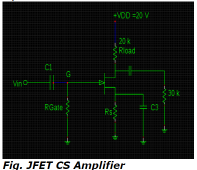
12) What is the voltage gain of below drawn JFET CS amplifier circuit whose transconductance and drain to source resistance values are 2000 μS & 200 k Ω respectively?
a. -56.56 V
b. 56.56 V
c. -36.36 V
d. 36.36 V
|
13) Which type of JFET amplifier circuit is also known as 'Source Follower' according to configurational strategic point of view?
a. Common Source amplifier
b. Common Drain amplifier
c. Common Gate amplifier
d. None of the above
|
14) The voltage gain of common drain JFET amplifier equals to unity only when ______.
a. gmrdRL >> (rd + RL)
b. gmrdRL << (rd + RL)
c. gmrdRL is exactly equal to (rd + RL)
d. gmrdRL ≠ (rd + RL)
|
15) Which is the most significant current generating parameter in common drain JFET amplifier?
a. gmVi
b. gmVgs
c. gmrd
d. gm (1 + Vgs)
|
16) Where is the current source connected in JFET common gate amplifier circuit configuration in the midst of input and output terminals so as to generate the gain of gmVgs?
a. between source and drain terminals
b. between gate and drain terminals
c. between source and gate terminals
d. between source, gate and drain terminals
|
17) Which MOSFET allows the flow of drain current even with zero gate to source voltage just due to existence of channel between drain and source terminals?
a. Depletion MOSFET
b. Enhancement MOSFET
c. Depletion-Enhancement MOSFET
d. All of the above
|
18) The enhancement type basically termed as normally-OFF MOSFET works only with _______.
a. large positive gate voltage
b. large negative gate voltage
c. large positive drain voltage
d. large negative drain voltage
|
19) Which property of MOSFET distinguishes it from JFET regarding to voltage application in addition to operational strategies and mechanisms?
a. Provision of applying positive and negative voltages to gate being insulated from channel
b. Provision of applying only positive voltage to gate to E-MOSFET
c. Provision of applying only negative voltage to gate to DE-MOSFET
d. All of the above
|
20) The depletion mode of MOSFET resemble semantically in the behaviour of JFET due to copious increase in ______.
a. negative gate voltage by reducing its conductivity level
b. negative gate voltage by enhancing its conductivity level
c. negative source voltage by reducing its conductivity level
d. negative source voltage by enhancing its conductivity level
|
Answer
Explanation
Related Ques
|
ANSWER: negative gate voltage by reducing its conductivity level
Explanation:
No explanation is available for this question!
|
|
21) The operation of De-MOSFET under the application of positive gate is also known as ________.
a. Depletion Mode
b. Enhancement Mode
c. Depletion-Enhancement Mode
d. None of the above
|
22) Which action plays a significant role in enhancing the conductivity of channel by inducing the free electrons especially in enhancement mode of N-channel MOSFET?
a. Inductor action
b. Capacitor action
c. Resistive action
d. Filter action
|
23) The input current of JFET and MOSFET are basically the leakage currents of ______ & ______ respectively
a. forward-biased PN junction & capacitor
b. reversed-biased PN junction & capacitor
c. forward-biased PN junction & inductor
d. reversed-biased PN junction & inductor
|
24) How is the layer of P-substrate, that intimate the provision of channel for electrons by touching substrate to metal -oxide film with the semantic behaviour of N-channel, can be referred as?
a. N-type Inversion layer
b. P-type Inversion layer
c. Both a & b
d. None of the above
|
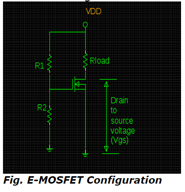
25) What is the computational the value of drain current for gate-to-source voltage (VGS) of about 6V in the below drawn schematic diagram of E-MOSFET along with ID(ON) = 2mA at VGS & VGS(threshold) of about 12V & 4V respectively?
a. 1 mA
b. 2 mA
c. 3 mA
d. 4 mA
|
26) Which mode is produced by a positive swing in gate-to-source voltage by input ac signal with the maximum voltage drop across load resistor in DE-MOSFET amplifier circuit?
a. Depletion mode with decrease in drain current
b. Enhancement mode with decrease in drain current
c. Depletion mode with an increase in drain current
d. Enhancement mode with an increase in drain current
|
Answer
Explanation
Related Ques
|
ANSWER: Enhancement mode with an increase in drain current
Explanation:
No explanation is available for this question!
|
|
27) FETs are widely applicable in oscilloscopes and voltmeters as an input amplifier as compared to bipolar transistors due to ______.
a. ability of minimizing the loading effect with high input resistance
b. ability of maximizing the loading effect with high input resistance
c. ability of minimizing the loading effect with low input resistance
d. ability of maximizing the loading effect with low input resistance
|
Answer
Explanation
Related Ques
|
ANSWER: ability of minimizing the loading effect with high input resistance
Explanation:
No explanation is available for this question!
|
|
28) How are the zener diodes placed internally in MOSFETs so as to provide defence from the hazardous consequences of stray voltages?
a. Alternately
b. Opposite to each other
c. Back-to-back
d. All of the above
|
29) How does the FET operate before the pinch-off region with small value of drain-to-source voltage in accordance to the control of drain-to-source resistance by the bias voltage?
a. As a Voltage Controlled Resistor
b. As a Voltage Dependent Resistor
c. As a Voltage-Variable Resistor
d. All of the above
|
30) The rectified & filtered signal taken at a high level point in AGC amplifier generates _______.
a. dc voltage proportional to the level of an output signal
b. dc voltage proportional to the level of an input signal
c. ac voltage proportional to the level of output signal
d. ac voltage proportional to the level of an input signal
|
Answer
Explanation
Related Ques
|
ANSWER: dc voltage proportional to the level of an output signal
Explanation:
No explanation is available for this question!
|
|
31) What is the major functioning role of VVR in the multistage AGC amplifier circuit during an increment in the signal level?
a. Variation in control of input signal level
b. Variation in voltage gain of multistage amplifier
c. Variation in current gain of multistage amplifier
d. Variation in control of output signal level
|
Answer
Explanation
Related Ques
|
ANSWER: Variation in voltage gain of multistage amplifier
Explanation:
No explanation is available for this question!
|
|


