1) What kind of waveforms are generated in UJT relaxation oscillator circuit due to additional involvement of external resistances in series configuration with the provision of corresponding base terminals?
a. Square waveforms
b. Triangular waveforms
c. Saw-tooth waveforms
d. Spike waveforms
|
Answer
Explanation
Related Ques
|
ANSWER: Spike waveforms
Explanation:
Relaxation oscillator basically comprises UJT and a capacitor that gets charged through resistance by switching ON VBB .
UJT fires when capacitor voltage reaches to the value of peak voltage in time 'ts' & immediately discharges till the voltage value decreases to lowermost value (Vv),
As a result, the device gets turned off and the capacitor begins to charge again and hence it leads to the repetition of cycle ceaselessly by generating sawtooth waveform across the capacitor.
In addition to this, the involvement of external resistances connected serially in the circuit results in the generation of spike waveforms despite of sawtooth, square or triangular ones.
|
|
2) What will be the requirement of maximum & minimum number of blades strokes per minute if UJT controls the motor of an automobile with stand-off ratio of about 0.7, capacitance of 40 μF and the charging resistances of 40 k & 480 k potentiometer connected in series combination?
a. 24 & 2.2 seconds respectively
b. 28 & 2.4 seconds respectively
c. 30 & 2.7 seconds respectively
d. 32 & 2.9 seconds respectively
|
Answer
Explanation
Related Ques
|
ANSWER: 30 & 2.7 seconds respectively
Explanation:
According to the given data,
Time constant has a least value of about 50000 x 40 x10-6 = 2 seconds
Considering the utilization of an entire potentiometer, the maximum value of this time constant is given by,
= (40 + 500) x 103 x 40 x 10-6
= 21.6 seconds
Maximum number of blade strokes per minute = 60 / 2 = 30 seconds
Minimum number of blade strokes per minute = 60 / 21.6 = 2.7 seconds
|
|
3) PUT gets turned ON only when there is an excession of ________ over the programmable level.
a. Anode voltage
b. Cathode voltage
c. Biasing voltage
d. Gate voltage
|
Answer
Explanation
Related Ques
|
ANSWER: Anode voltage
Explanation:
Programmable UJT (PUT) is also PNPN device comprising four layers along with terminal connected to N-region adjacently to anode & also exhibit similar V-I characteristics as that of UJT.
This PN junction undergoes in forward biased mode whenever the value of anode voltage goes beyond the gate voltage by 0.7 V, by ultimately turning ON the PUT.
On the contrary, the PUT gets turned OFF when the value of anode voltage decreases below this level.
The condition at which the anode voltage crosses this level is an eventual stage of turning ON the PUT & also the level is termed as programmable level.
Besides this, gate biasing can be adjusted to any desired level with an assistance of externally connected voltage-divider circuit and hence it is completely independent of programmable level.
|
|
4) What is the value of anode current of SCR comprising two-transistor analogy with the gate current of 40 mA if the gain of PNP & NPN transistors are 0.3 & 0.4 respectively?
a. 253 mA
b. 113 mA
c. 73.33 mA
d. 53.33 mA
|
Answer
Explanation
Related Ques
|
ANSWER: 53.33 mA
Explanation:
According to given data:
Gain of PNP transistor = a1 = 0.3
Gain of NPN transistor = a2 = 0.4
Gate current = IG = 40 mA = 0.04 A
According to the formula of anode current,
Anode current = IA = a2 IG / [1- (a1 + a2 )]
= (0.4 x 0.04 ) / [1 - (0.3 + 0.4)]
= 0.016 / 0.3
= 53.33 mA
|
|
5) Which thyristor behaves like two SCRs connected in parallel configuration & upside down corresponding to each other?
a. Diac
b. Triac
c. LASCR
d. Shockley Diode
|
Answer
Explanation
Related Ques
|
ANSWER: Triac
Explanation:
Triac is a bi-directional device comprising 5 layers and two SCRs connected in parallel combination upside down with respect to each other. This implies that the anode of one SCR is connected to the cathode of the other and the associated gates are directly connected together. Hence, it is possible to trigger the triac into conduction by both positive and negative voltages at its anodes as well as with both positive and negative triggering pulses at its gate.
Control of ac power supplied to load by switching ON & OFF modes during positive and negative half cycles is the major application of triac but is limited to the use of ac supply frequencies upto 400 Hz since it consumes more duration to recover to OFF state.
|
|
6) Determine the input voltage necessary to cause the breakdown in SCR for 200 Ω resistance connected in series if the required gate current for firing is 6 mA.
a. 2.7 V
b. 2.9 V
c. 1.9 V
d. 1.2 V
|
Answer
Explanation
Related Ques
|
ANSWER: 1.9 V
Explanation:
In accordance to the given data, it is mandatory to estimate the value of input voltage in such a manner that it should overcome the barrier voltage of 0.7 V.
Secondly, it should allow the current of 6 mA to flow through the resistor of about 200 Ω.
Hence, the value of input voltage can be estimated as,
Input Voltage = Gate to Cathode Voltage + (Gate Current x Resistance)
Thus, Vin = VGC + IG R
= 0.7 +( 6 x 10-3 x 200 )
= 0.7 + (1200 x 10-3 )
= 1.9 V
|
|
7) A device which possesses the potential to convert a sinusoidal input waveform (zero average value) into a unidirectional waveform with a non-zero average component is known as ___________
a. Inverter
b. Rectifier
c. Chopper
d. Clamper
|
Answer
Explanation
Related Ques
|
ANSWER: Rectifier
Explanation:
Rectification is the process of converting AC to DC & basically diode act as a rectifier. Rectifier is a circuit which comprises one or more diodes so as to convert ac voltage into pulsating dc voltage.
On the contrary, inverter plays a crucial role in converting dc to ac. Chopper performs the functioning of DC to DC conversion while clamper circuits introduces a DC level into an ac signal & usually referred as DC restorers.
|
|
8) Determine the voltage regulation and efficiency of a half-wave rectifier circuit that uses silicon diode with a forward resistance of 0.15 ohm, load resistance of 15 ohm, threshold voltage of about 0.7 V and emf at secondary winding is about 16 Vrms including the emf resistance of about 0.4 ohm.
a. 4.8% & 36.06%
b. 1.2% & 36.06%
c. 2.5% & 42.06%
d. 3.6% & 42.06%
|
Answer
Explanation
Related Ques
|
ANSWER: 3.6% & 42.06%
Explanation:
Considering the half-wave rectifier circuit,
Voltage Regulation (VR) = R0 / RL
But, Ro = emf resistance + forward resistance
= 0.4 + 0.15
= 0.55
VR = R0 / RL
= 0.55 / 15 = 0.036 or 3.6 %
Efficiency (η) = Pdc / Pin = 40.6 / (1 + Ro / RL )
= 40.6 (1 + 0.55 / 15)
= 42.06 %
|
|
9) Which parameter plays a cardinal role in determining the ratings of transformer while designing any power supply?
a. Ripple Factor
b. Transformer Utilization Factor (TUF)
c. Peak Inverse Voltage
d. Efficiency
|
Answer
Explanation
Related Ques
|
ANSWER: Transformer Utilization Factor (TUF)
Explanation:
While designing any regulated or unregulated type of power supply, it is extravagantly essential to estimate the ratings of transformer in terms of Transformer Utilization Factor (TUF).
TUF can be evaluated on the basis of the quantity of power delivered to load as well as the type of rectifier circuit employed by it. Simply, it can be defined as :
TUF = dc power delivered to load / ac rating of transformer secondary
= Pdc / Pac . Rated
It is slightly different from conversion efficiency. Conversion efficiency measures the ratio of output dc power to total amount of input power.
η = Pdc / Pin
Apart from these, peak inverse voltage is the maximum voltage that occurs across the rectifying diode in reverse direction; while ripple factor can be defined in terms of rms value of ac voltage to that of the dc load voltage.
|
|
10) The significant reason(s) for using bridge wave rectifier is (are)
a. Less PIV rating
b. No necessity of centre - tap winding usage
c. Suitability for high voltage applications
d. All of the above
|
Answer
Explanation
Related Ques
|
ANSWER: All of the above
Explanation:
Full-wave bridge rectifier circuit consists of four diodes without the necessity of centre- tapped transformer winding. In addition to this, small transformers are sufficient to utilize for controlling the same output level despite of using large transformers as in case of full-wave rectifier circuits with two diodes. Less PIV rating per diode is another important characteristic feature that serves to be quite beneficiary.
However, it becomes more flexible and easier to perform the rectification level by preferring full wave bridge rectifiers especially for high voltage applications.
|
|
11) What is / are the possible consequences of increasing the filter capacitance?
a. Reduction in magnitude of ripple voltage
b. Reduction in peak current of diode
c. Reduction in Vdc towards the limiting value Vip
d. All of the above
|
Answer
Explanation
Related Ques
|
ANSWER: Reduction in magnitude of ripple voltage
Explanation:
Basically, a capacitor opposes the change in voltage. The main function of filter circuit is to convert a pulsating output from a rectifier into a steady dc level since it smoothens out the pulstations at the output. A bigger capacitor is more likely to minimize the content or magnitude of ripple voltage.
With an increase in capacitor size, the peak current in the diode and dc voltage towards its limiting value also increases whereas magnitude of ripple voltage along with the time of flow current pulse in the diode goes on decreasing.
|
|
12) The conduction angle in controlled rectification process under the proper firing conditions can be controlled by _______
a. Thyristor
b. Rectifier
c. Comparator
d. Regulator
|
Answer
Explanation
Related Ques
|
ANSWER: Thyristor
Explanation:
Controlled rectification process allow to vary the output of rectifier by controlling the point in ac cycle where the circuit gets turned ON during specific firing conditions. Thyristor like SCR is specifically used to control ( or trigger) the level of conduction angle in the cycle under the proper firing conditions. Only under the application of control signal to turn on the rectifier at a particular point, the load current flows through an ac cycle.
However, an half wave rectifier remains in conduction phase for the remaining positive half-cycle.
Due to this, determination of firing point is possible by an angle of delay while the firing signal is applied by the control circuit. Increase in delay angle ultimately results in delay of conduction phase in the cycle along with the decrement in load current.
|
|
13) Estimate the power delivered to the load circuit for firing angles of 450 & 900 respectively in a controlled form of half-rectifier circuit with peak supply voltage of about 300 V across the load resistor of 2 kΩ.
a. 0.502 W & 0.244 W respectively
b. 1.240 W & 0.062 W respectively
c. 2.120 W & 1.670 W respectively
d. 3.240 W & 1.097 W respectively
|
Answer
Explanation
Related Ques
|
ANSWER: 3.240 W & 1.097 W respectively
Explanation:
> Given data:
Vm = 300 V , RL = 2 kΩ
For θ = 450 , the power delivered can be given by,
P = Vdc x Idc
But, for a half-wave controlled rectifier,
Vdc = Vm / 2Л (1 + cos θ )
= Vm / 2Л (1+ cos 45)
= Vm / 2Л ( 1+ 0.707)
Vdc = 0.27 Vm
= 0.27 x 300
Vdc = 81 V
Idc = Vdc / RL = 81 / 2000 = 40 mA
Therefore, P = Vdc x Idc = 81 x 40 = 3240 mW = 3.240 W
Similarly, the power delivered at an angle θ = 900 can be estimated as,
Vdc = Vm / 2Л (1 + cos θ )
= Vm / 2Л (1 + cos 900)
= Vm / 2Л (1 + 0)
= Vm / 2Л
= 0.159 Vm
= 0.159 x 300
Vdc = 47.7 V
Idc = Vdc / RL = 47.7 / 2000 = 23 mA
Hence, P = Vdc x Idc = 47.7 x 23 = 1097.1mW = 1.097 W
|
|
14) What will be the average dc output voltage of a chopper which is supplied by 500 V dc with ON time of 20ms and OFF time of 15 ms?
a. 150 V
b. 230 V
c. 285 V
d. 325 V
|
Answer
Explanation
Related Ques
|
ANSWER: 285 V
Explanation:
According to given data,
TON = 20 ms = 20 x 10 -3 s
TOFF = 15 ms = 15 x 10 -3 s
T = TON + TOFF
T = (20 x 10 -3 + 15 x 10 -3 ) = 35 x 10-3 s
Therefore, duty cycle of the chopper is given by,
T = TON / T = 20 x 10 -3 / 35 x 10-3 = 0.57
Thus, average dc output voltage of chopper can be evaluated by,
VL = Vdc x duty cycle = 500 x 0.57 = 285 V
|
|
15) Which component reduces the difference between no load and full load voltage by ameliorating the regulation when connected across the output of filter?
a. Shunt Capacitor
b. Series Inductor
c. Bleeder Resistor
d. Silicon Controlled Rectifier
|
Answer
Explanation
Related Ques
|
ANSWER: Bleeder Resistor
Explanation:
Bleeder resistor is most often configured across the output of filter so as to improve or enhance the voltage regulation. This resistor results in initial voltage drop by acting as a pre-load on the supply. Therefore, small amount of additional voltage drop gets generated due to connection of real load in the circuit configuration.
Thus, it becomes easier to figure the difference between no-load and full-load voltage and ultimately reduce it by improving the regulation level. Bleeder resistor renders a path for filter capacitor for discharging purpose in the absence of power supply ( or when power supply is switched off) and hence it is generally referred as a 'Bleeder Resistor'.
One major advantage of the bleeder resistor is that it invigorates the capability to improve the filtering action by controlling minimum current through the choke.
|
|
16) Which filter circuit is most often and specifically used with low current equipment in order to prevent the rectifier diodes from damage of high peak current pulses?
a. R-C Filter
b. C-L-C Filter
c. L-C Filter
d. Series Inductor Filter
|
Answer
Explanation
Related Ques
|
ANSWER: C-L-C Filter
Explanation:
C-L-C filter (or Pi- filter) comprises one inductor and two capacitors connected in Л configuration. Hence, it is also known as capacitor input Л filter.
The function of filtering is more better as compared to L-C filter circuit. Generally, the connection of capacitor C1 is configured directly across the supply.
Due to this, the necessity of high pulse current arises because of the generation of load current to greater extent.
The presence of these high peak current pulses may prove to be pernicious to damage the rectifier diode.
However, it is obligatory for C-L-C filters to be conditionally used with low-current equipment.
|
|
17) The voltage across the current sensing resistor in switching voltage IC regulators is used internally by an oscillator to make variations in the duty cycle on the basis of desired ________
a. Peak Voltage
b. Peak Current
c. Peak Frequency
d. Pulse- Width
|
Answer
Explanation
Related Ques
|
ANSWER: Peak Current
Explanation:
The output voltage is always greater than the input voltage for an IC connected to external components under the category of step-up switching regulator configuration. Pulse – width and frequency of an oscillator used in regulatory circuit are controlled by timing capacitor (CT) .
Variations in duty-cycle can be controlled only on the basis of desired peak current and completely independent of peak voltage. This is so because the necessary voltage required by an oscillator internally is generally obtained across the current sensing resistor. Eventually, the regulating action is in addition and accordance to the output produced by the variations exhibited in duty-cycle of an oscillator.
|
|
18) Which circuit has the potential to overcome the drawback of unprotected external pass transistor from the excessive current from a shorted output in linear voltage regulators?
a. Current Regulator
b. Current Limiter
c. Voltage Regulator
d. Voltage Limiter
|
Answer
Explanation
Related Ques
|
ANSWER: Current Limiter
Explanation:
The current sensing resistor sets base-to-emitter voltage of transistor in current-limiting circuit, by evaluating the difference between the voltage across the external resistor and voltage across limiting resistor due to opposite polarities. If the value of current through the external pass transistor increases beyond maximum value due to shorted output, then the value of voltage across the limiting resistor reaches to 0.7V by turning ON the current limiting transistor.
Hence, it becomes feasible for the current limiting transistor to conduct the current away from the external pass transistor as well as regulator. This ultimately results in an occurrence of thermal overload to some extent by shutting down the regulator. Factually, overall internal protection of IC voltage regulator from thermal overload is a major stage taken into consideration from designing point of view.
|
|
19) What is the maximum and minimum output voltages for IC voltage regulator shown below if adjustable current and input voltage are 98.5μA and 40 V respectively with the variable range of resistances from zero to 5 k ohm ?
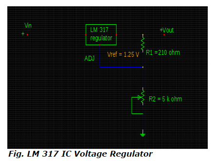
a. 30.16 V & 1.25 V
b. 29.66 V & 0 V
c. 27.99 V & 0 V
d. 31.49 V & 1.25 V
|
Answer
Explanation
Related Ques
|
ANSWER: 31.49 V & 1.25 V
Explanation:
According to the equation of output voltage for IC voltage regulator,
Vout = Vref [1+ (R2/ R1)] + IADJ R2
Considering R2 at its minimum value = 0 ohm, the output voltage is evaluated by,
Vout (min) = 1.25 [1 + (0 / 210 )] + (98.5 x10-6) x 0
= 1.25 V
For maximum value of R2 = 5 k ohm, the output voltage is,
Vout (max) = 1.25 [1 + (5 x 10³ / 210)] + (98.5 x 10⁻⁶ ) x 5 x 103
= 1.25 [1+ (5000 / 210)] + (98.5 x 10 - 6) x 5000
= 31 + 0.4925
= 31. 49 V
|
|
20) Which kind of switching regulator has a distinct characteristic of generating the output voltage always less than input voltage where the variations in output voltage can be undertaken by adjusting duty-cycle of transistor?
a. Step- Up Regulator
b. Step-Down Regulator
c. Inverting Regulator
d. None of the above
|
Answer
Explanation
Related Ques
|
ANSWER: Step-Down Regulator
Explanation:
Non-inverting Regulator
The output voltage in step-down regulator mainly depends on input voltage and pulse-width. Pulse width refers to ON time of transistor. With an increase in ON-time relative to OFF-time, charging capacity of capacitor increases by simultaneously increasing the output voltage & vice-versa. Hence, a wide range of variation can be observed in output voltage by adjusting the duty-cycle ( the ratio of TON / T ) of the transistor by,
VOUT = Vin (TON / T)
where, the 'T' represents the period of ON-OFF cycle of transistor & has a reciprocal relative significance with the frequency in the form of T = 1 / f
Also, Total T = TON + TOFF & hence the ratio of TON / T is precisely known as 'Duty Cycle'.
|
|


