Basic Electronics Engineering - Electronic Engineering (MCQ) questions & answers
Dear Readers, Welcome to Basic Electronics Engineering multiple choice questions and answers with explanation. These objective type Basic Electronics Engineering questions are very important for campus placement test, semester exams, job interviews and competitive exams like GATE, IES, PSU, NET/SET/JRF, UPSC and diploma.
Specially developed for the Electronic Engineering freshers and professionals, these model questions are asked in the online technical test and interview of many companies.
These tutorial are also important for your viva in university exams like Anna university, Pune, VTU, UPTU, CUSAT etc.
1) What is the major functioning role of VVR in the multistage AGC amplifier circuit during an increment in the signal level?
- Published on 30 Oct 15
a. Variation in control of input signal level
b. Variation in voltage gain of multistage amplifier
c. Variation in current gain of multistage amplifier
d. Variation in control of output signal level
|
Answer
Explanation
Related Ques
|
ANSWER: Variation in voltage gain of multistage amplifier
Explanation:
No explanation is available for this question!
|
|
2) The rectified & filtered signal taken at a high level point in AGC amplifier generates _______.
- Published on 30 Oct 15
a. dc voltage proportional to the level of an output signal
b. dc voltage proportional to the level of an input signal
c. ac voltage proportional to the level of output signal
d. ac voltage proportional to the level of an input signal
|
Answer
Explanation
Related Ques
|
ANSWER: dc voltage proportional to the level of an output signal
Explanation:
No explanation is available for this question!
|
|
3) How does the FET operate before the pinch-off region with small value of drain-to-source voltage in accordance to the control of drain-to-source resistance by the bias voltage?
- Published on 30 Oct 15
a. As a Voltage Controlled Resistor
b. As a Voltage Dependent Resistor
c. As a Voltage-Variable Resistor
d. All of the above
|
4) How are the zener diodes placed internally in MOSFETs so as to provide defence from the hazardous consequences of stray voltages?
- Published on 30 Oct 15
a. Alternately
b. Opposite to each other
c. Back-to-back
d. All of the above
|
5) FETs are widely applicable in oscilloscopes and voltmeters as an input amplifier as compared to bipolar transistors due to ______.
- Published on 30 Oct 15
a. ability of minimizing the loading effect with high input resistance
b. ability of maximizing the loading effect with high input resistance
c. ability of minimizing the loading effect with low input resistance
d. ability of maximizing the loading effect with low input resistance
|
Answer
Explanation
Related Ques
|
ANSWER: ability of minimizing the loading effect with high input resistance
Explanation:
No explanation is available for this question!
|
|
6) Which mode is produced by a positive swing in gate-to-source voltage by input ac signal with the maximum voltage drop across load resistor in DE-MOSFET amplifier circuit?
- Published on 30 Oct 15
a. Depletion mode with decrease in drain current
b. Enhancement mode with decrease in drain current
c. Depletion mode with an increase in drain current
d. Enhancement mode with an increase in drain current
|
Answer
Explanation
Related Ques
|
ANSWER: Enhancement mode with an increase in drain current
Explanation:
No explanation is available for this question!
|
|
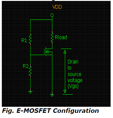
7) What is the computational the value of drain current for gate-to-source voltage (VGS) of about 6V in the below drawn schematic diagram of E-MOSFET along with ID(ON) = 2mA at VGS & VGS(threshold) of about 12V & 4V respectively?
- Published on 30 Oct 15
a. 1 mA
b. 2 mA
c. 3 mA
d. 4 mA
|
8) How is the layer of P-substrate, that intimate the provision of channel for electrons by touching substrate to metal -oxide film with the semantic behaviour of N-channel, can be referred as?
- Published on 30 Oct 15
a. N-type Inversion layer
b. P-type Inversion layer
c. Both a & b
d. None of the above
|
9) The input current of JFET and MOSFET are basically the leakage currents of ______ & ______ respectively
- Published on 30 Oct 15
a. forward-biased PN junction & capacitor
b. reversed-biased PN junction & capacitor
c. forward-biased PN junction & inductor
d. reversed-biased PN junction & inductor
|
10) Which action plays a significant role in enhancing the conductivity of channel by inducing the free electrons especially in enhancement mode of N-channel MOSFET?
- Published on 30 Oct 15
a. Inductor action
b. Capacitor action
c. Resistive action
d. Filter action
|


