Combinational Circuits and Sequential Circuits
Construct 3×8 decoder and explain its truth table.
Decoder- A decoder is a device that creates a large no. of outputs taking the lesser no. of inputs.
- It is also called as a de-multiplexer.
3×8 DecoderAs we have just seen that a decoder takes lesser inputs and provides more no. of outputs. In a 3×8 decoder three inputs are taken and 8 outputs are provided out of them.
- Its outputs are active- high, so it uses AND gates.
- It has three input lines and eight output lines.
- It is called as a binary to octal decoder.
- It takes a 3-bit binary input code and activates one of the 8 outputs corresponding to that code.
Diagram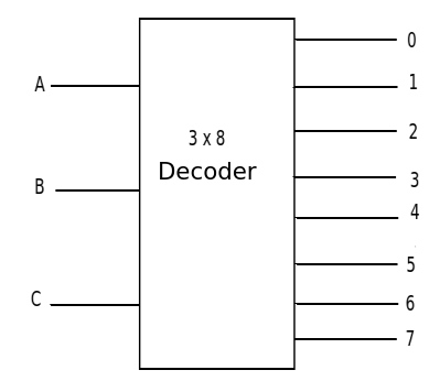 Truth Table
| A | B | C | Z |
|---|
0
0
0
0
1
1
1
1 | 0
0
1
1
0
0
1
1 | 0
1
0
1
0
1
0
1 | 1
0
1
0
0
1
0
0 |
Construct JK flip-flop and describe its functions.
- The JK flip-flop is the most widely used flip-flop design.
Few of its features are- It is considered to be a universal flip-flop circuit.
- “JK flip flop” has no invalid input states even when S and R are both at logic “1”.
- It can be said as a gated SR flip flop.
Working of a JK flipflop (its functioning)- The JK flip-flop consists of two inputs: J and K and one clock input.
- There are two outputs Q and Q' and here Q' is the reverse of Q.
Diagram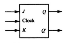 Operational Diagram
| J K | OUTPUT |
|---|
0 0
0 1
1 0
1 1 | Q
1
0
Q' |
The above diagram explains the following points:- When J=0 and K=0, the current output will move to the next state.
- When J=0 and K=1, the output of the next state will be put to 0.
- When J=1 and K=0, the output of the next state will be put to 1.
- When J=1 and K=1, the output of the next state will be the inverse of the output of current state.
Construct 1 × 8 De-multiplexer and explain it with truth table.
- A 1 × 8 De-multiplexer is the one which takes in single input and provides 8 outputs.
- It provides 3 input signals, decodes them and then selects one out of the eight mutually exclusive outputs.
- The two out of the three inputs are active high and the remaining one is active low.
- F138 is one of the high speed 1x8 decoder.
Diagram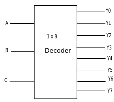 Truth Table
| A | B | C | Y0 | Y1 | Y2 | Y3 | Y4 | Y5 | Y6 | Y7 |
|---|
0
0
0
0
1
1
1
1 | 0
0
1
1
0
0
1
1 | 0
1
0
1
0
1
0
1 | 0
0
0
0
0
0
0
1 | 0
0
0
0
0
0
1
0 | 0
0
0
0
0
1
0
0 | 0
0
0
0
1
0
0
0 | 0
0
0
1
0
0
0
0 | 0
0
1
0
0
0
0
0 | 0
1
0
0
0
0
0
0 | 1
0
0
0
0
0
0
0 |
Construct D-flip flop and describe its functions.
The drawback of the SR NAND Gate, that its indeterminate input condition SET = 0 and RESET = 0 is forbidden and it results in both outputs to be at logic “1”, over-riding the feedback latching action, which make any input going to logic level “1” first will lose control, while the other input still be “0” marked the construction of D flipflop. In this an inverter is connected between the SET and RESET inputs which gives another type of flip flop circuit known as
D-type Flip Flop.
So, a D-type flip flop- Ensures that inputs S and R are never “1” at the same time.
- Constructed from a gated SR flip-flop by adding an inverter in between.
- Most important application of the D flip flop is as a Data Latch.
- Majorly called as Delay flip flop, Data flip flop.
Diagram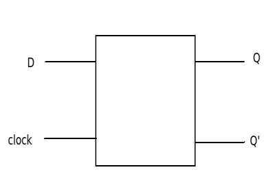
- The above diagram shows a D flipflop with one input and two outputs.
- It always provide outputs Q and Q' (inverted) and ensures that they are never on same logic.
Write a short note on the type of registers used in microprocessors.
- Register plays a major role in CPU operations.
- They contain a set of binary storage cells called the flip-flops with reading or writing or both the facilities.
- The number of bits in a register depends on the type of data and its address. During the execution of a process, the microprocessors picks up the instructions from one register and gives it to other for performing the tasks and at last stores it on another register.
There are two basic type of registers that the microprocessors use:1. MAR (Memory Address Register)- It holds the memory addresses of data and instructions.
- It is used to store the address of the instructions that are used during the execution phase of the process.
2. Program Counter- The program counter is a processor register.
- It is also known as instruction pointer (IP) it keeps track of the next instruction to be executed by keeping in track its memory address.
- Its a 16-bit register.
3. Accumulator Register- It accumulates (stores) the results that the system has produced.
4. Index Register- Also known as base register.
- It holds a number that can be added to make an accurate memory address.
5. MBR- It stands for Memory Buffer Register.
- This register stores the contents of data or instructions that are coming from or going to the memory.
6. Data Register- This register is used by microcomputers to temporarily store data coming from or going to a peripheral device.


